Comparison map
Semiconductor Electronics: relationships and examples
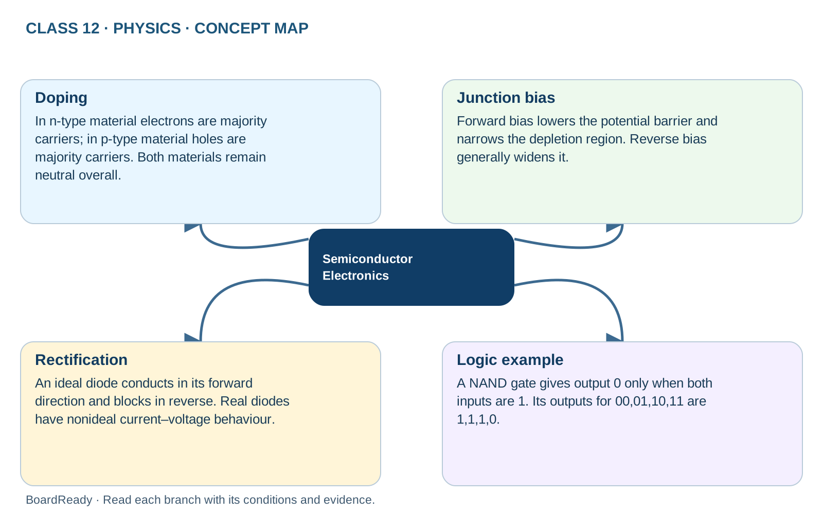
Relate carriers, junction bias and device function without confusing ideal and real models. Doping: In n-type material electrons are majority carriers; in p-type material holes are majority carriers. Both materials remain neutral overall. Junction bias: Forward bias lowers the potential barrier and narrows the depletion region. Reverse bias generally widens it. Rectification: An ideal diode conducts in its forward direction and blocks in reverse. Real diodes have nonideal current–voltage behaviour. Logic example: A NAND gate gives output 0 only when both inputs are 1. Its outputs for 00,01,10,11 are 1,1,1,0.Exam cue: Use a stated diode model. Doping changes carrier populations, not the net charge of a bulk sample.
- 1Semiconductor Electronics -> Doping: In n-type material electrons are majority carriers; in p-type material holes are majority carriers. Both materials remain neutral overall.
- 2Semiconductor Electronics -> Junction bias: Forward bias lowers the potential barrier and narrows the depletion region. Reverse bias generally widens it.
- 3Semiconductor Electronics -> Rectification: An ideal diode conducts in its forward direction and blocks in reverse. Real diodes have nonideal current–voltage behaviour.
- 4Semiconductor Electronics -> Logic example: A NAND gate gives output 0 only when both inputs are 1. Its outputs for 00,01,10,11 are 1,1,1,0.